The construction of Samsung Electronics's new semiconductor R & D center began today, and Li's first public agenda after the amnesty.
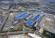
CTOnews.com August 19 news, Samsung today in Yongin City, Gyeonggi Province, South Korea, held a new semiconductor research and development (R&D) center groundbreaking ceremony.
Covering an area of approximately 109000 square meters, the research center was established to advance Samsung's memory, system semiconductor and foundry technologies.
CTOnews.com learned that this is Lee Jae-yong's first public schedule since he was pardoned and returned to the front line of business on Recovery Day.
He said that it has been 40 years since the company broke ground on its semiconductor plant, and today it begins a new challenge again. Without bold investment in R & D, Samsung Semiconductor would not be where it is today. Let us continue the tradition of "valuing technology and investing first" and create the future with unprecedented new technologies.
According to reports, the park is Samsung Electronics 'new R & D center in China eight years after 2014. Samsung Electronics said that if a research and development center with cutting-edge equipment is built, it is expected to shorten the development time of new generation products and improve semiconductor quality.
Samsung Electronics said it plans to invest 20 trillion won (about 102.6 billion yuan) to build new facilities by 2028 and will use the new complex as a research center for system chips. By 2025 the central complex will have exclusive assembly lines.