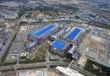
Samsung Electronics will build a chip development facility in Japan, with an estimated investment of more than 30 billion yen
CTOnews.com, May 14 (Xinhua) Samsung Electronics will build a new development facility in Yokohama, a symbolic move that is expected to promote cooperation between the chip industry in Japan and South Korea, according to the Nikkei News.
It is said that the new chip development facility, which will cost more than 30 billion yen (CTOnews.com Note: currently about 1.545 billion yuan), will be built in Yokohama, southwest of Tokyo, which is also home to Samsung Japan Research Institute. The facility will focus on "back-end" production, that is, packaging wafers into final products.
In fact, in March this year, it was announced that Samsung had merged two R & D facilities in Yokohama and Osaka and would create an integrated R & D center in Japan called DSRJ, which is located in Samsung's Yokohama Research Institute.
At the time, Samsung said the main reason for merging the two R & D centers was the rapprochement between South Korea and Japan, hoping to build a new semiconductor and display R & D center in Japan.
In addition, Samsung hopes to set up a new comprehensive research center for Device eXperience, its device experience unit, in Japan under the name of "Samsung Research Japan". Foreign media believe that Samsung is trying to enhance its comprehensive development capability by reorganizing R & D institutions related to device solutions.